NEC develops the world’s first content addressable memory that stores data without using power and it akes data deposits sans power, RAM green with envy. New content addressable memory promises five-nanosecond retrieval speeds equal to sticks of DDR3 1600 and can store data even when the power’s off. Spintronics logic is what makes the magic happen by setting the spin direction of electrons and using their interaction with magnetic forces to store bits of data and those spinning attributes are then kept on the circuit even when there’s no electricity flowing………..
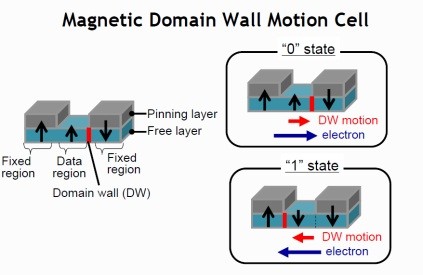
NEC Corporation (NEC) and Tohoku University announced the development of the world’s first content addressable memory (CAM) that both maintains the same high operation speed and non-volatile operation as existing circuits when processing and storing data on a circuit while power is off. NEC‘s new CAM is a part of spintronics logic integrated circuit technologies that utilize the negative properties of electrons together with the spin magnetic moment. The new CAM utilizes the vertical magnetization of vertical domain wall elements in reaction to magnetic substances in order to enable data that is processing within the CAM to be stored on a circuit without using power. This contrasts to conventional technologies that required data to be stored within memory. As a result, data can be saved on circuits even when power is cut from the CAM. In recent years, the use of ICT equipment has steadily increased due to the widespread growth of cloud computing. Most existing equipment requires a short amount of time to get started and internal circuits remain active when the equipment is in standby mode. Therefore, the growing consumption of power by ICT equipment in standby mode has become a serious concern.
Use of the new CAM in combination with existing nonvolatile memory is related to greater non-volatility of CPU for electronics and other storage devices. Furthermore, use of this new CAM enables the development of electronics that start instantly and consume zero electricity while in standby mode. In order for CAM to be both nonvolatile and maintain a high speed, two spintronics devices, spinning in opposite directions to one another, were connected within the same cell. In terms of constructing the circuit, writing is done once by connecting two devices in a series using recently developed three pin particles that separate the current path into writing and reading. This new process enables cells to become more compact since the number of writing switches per element is reduced by one. Moreover, the new CAM achieve the same level of high-speed data retrieval as current CMOS based CAM that feature 5ns and low power consumption of 9.4mW.
Approximately half the circuit area in comparison to existing technologies. In addition to the vertical domain wall element can connect in series by separating the route of current into reading and writing, the newly developed CAM circuit technologies can reduce the number of transistors from eight to three in every two cells by sharing transistors. This results in a 50% CAM area reduction. NEC developed nonvolatile particles aiming for both greater convenience and energy conservation. Additionally, NEC and Tohoku University developed a simulation technology for a circuit diagram including spintronics particles in parallel with designing technologies for massively large integrated circuits for developments involving the most advanced spintronics logic integrated circuits. Looking forward, NEC and Tohoku University will continue to drive the latest developments of integrated circuits that capitalize on spintronics technology. NEC and Tohoku University will announce their latest results on June 17 at VLSI Circuit Symposium 2011 (June 13-17, Kyoto).
[ttjad keyword=”processor”]