South Korean electronics-giant Samsung, a global leader in advanced semiconductor solutions, announced on Thursday that it reached another milestone in the development of 14nm FinFET process technology with the successful tape-out of multiple development vehicles in collaboration with its key design and IP partners. The new design promises to offer substantial power and performance improvements compared to existing designs.
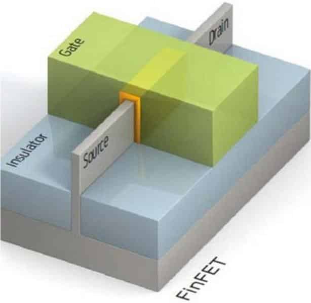
Samsung has achieved a “successful tape out of multiple development vehicles” for its 14nm process. Now the company is collaborating with “key design and IP partners” like ARM to pursue 14nm process technology. 14nm process technology is the successor of the current 22nm processes that are used to manufacture chips for PCs, servers, mobile devices, embedded systems, and other computational hardware.
Samsung, ARM, and additional ecosystem partners Cadence, Mentor, and Synopsys, recently have taped out a “full ARM Cortex-A7 processor” using the 14nm process. According to Samsung, the Cortex-A7 tape-out is “a significant milestone for silicon manufacturing for the fabless ecosystem.” The partners have already made a 14nm process design kit (PDK) which is available to fabless chip design companies that license ARM designs.
Samsung believes that 14nm process will provide major advantages to future-generation System-on-a-Chip (SoC) devices used in smartphones, tablets, and other consumer electronics products.
Source: Samsung
Thanks To: PC Magazine, X-bit Laboratories
[ttjad keyword=”samsung-laptop”]