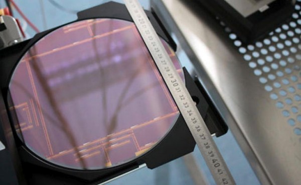
World’s biggest CMOS sensor could help doctors detect and heralds better treatment for cancer patients.Measuring a hefty 12.8 square cm, DyNAMITe is roughly 200 times bigger than the chips you’d find in most PCs, making it the largest imager ever made on a wafer of standard and this extra girth allows the active pixel sensor to capture images in high detail with a 100-micrometer pitch boasting 1280 x 1280p aligned next to a 50-micron layer, carrying 2560 x 2560p………
Scientists at the University of Lincoln have created the world’s biggest microchip designed for medical imaging.The 12.8 cm square chip means that in future doctors will be able to diagnose cancer and see the impact of radiotherapy treatment far more precisely than ever before.A consortium led by Nigel Allinson, Distinguished Professor of Image Engineering at Lincoln, created “DynAMITe“, the wafer-scale chip that is 200 times larger than the processing chips that lie at the heart of current PCs and laptops.The images it produces will show very clearly the impact of radiation on tumours as well as aid the detection in the earliest stages. It is also super-strong, being able to survive many years of exposure to radiation.Prof Allinson said: “DynAMITe was designed for medical imaging, in particular mammography and radiotherapy, so the individual pixels are much larger than those found in consumer digital cameras or mobile phones. As it will withstand exposure to very high levels of x-ray and other radiation, it will operate for many years in the adverse environment of cancer diagnosis and treatment instruments; and represents a major advance over the existing technology of amorphous Silicon panels.”
The project has been funded by the UK Engineering and Physical Sciences Research Council and involves medical physicists at The Institute of Cancer Research (ICR) and The Royal Marsden Hospital, who are investigating potential applications for the technology.“Our clinical work has given us an insight into areas in which the existing technology falls short, and we were very pleased the consortium was able to design a microchip that met our exact specifications for medical imaging,” says Professor Phil Evans from the ICR. “We are looking forward to investigating all the potential uses for this chip in cancer research and treatment.””Our clinical work has given us an insight into areas in which the existing technology falls short, and we were very pleased the consortium was able to design a microchip that met our exact specifications for medical imaging,” says Professor Phil Evans from the ICR. “We are looking forward to investigating all the potential uses for this chip in cancer research and treatment.”This was one of the challenges set in the Research Council’s Roadmap of the major research challenges facing the microelectronics industry. The 12.8 cm square imager is the largest device that can be made on a single industry standard eight inch (20 cm) diameter wafer.
The MI-3 Plus consortium consists of medical /life science physicists and engineers from University College London, Institute of Cancer Research (Royal Marsden Hospital) and the University of Surrey as well as the microelectronics design resources at the University of Lincoln.The MI-3 Plus Consortium members are Professor Nigel M Allinson, Dr Thalis Anaxagoras (University of Lincoln), Professor Robert Speller (University College, London), Professor Phil Evans (The Institute of Cancer Research), and Dr Kevin Wells and Dr Michela Esposito (University of Surrey).Funded by the UK Engineering and Physical Sciences Research Council under their Basic Technology Translation Grant Scheme.
[ttjad keyword=”general”]


