IBM believes a new way of encoding the bits in phase-change memory will it reliable enough for use in servers and developed a programming trick that makes it possible to more reliably store large amounts of data using a promising new technology called phase-change memory. It means scientists are one step closer to creating a universal memory chip that is fast, permanent, and has lots of capacity and these multi-bit phase-change memory chips could transform enterprise computing and storage by around 2016…………
For the first time, scientists at IBM Research have demonstrated that a relatively new memory technology, known as phase-change memory (PCM) and it can reliably store multiple data bits per cell over extended periods of time. This significant improvement advances the development of low-cost, faster and more durable memory applications for consumer devices, including mobile phones and cloud storage, as well as high-performance applications, such as enterprise data storage. With a combination of speed, endurance, non-volatility and density, PCM can enable a paradigm shift for enterprise IT and storage systems within the next five years. Scientists have long been searching for a universal, non-volatile memory technology with far superior performance than Flash, today’s most ubiquitous non-volatile memory technology. The benefits of such a memory technology would allow computers and servers to boot instantaneously and significantly enhance the overall performance of IT systems. A promising contender is PCM that can write and retrieve data 100 times faster than Flash, enable high storage capacities and not lose data when the power is turned off. Unlike Flash, PCM is also very durable and can endure at least 10 million write cycles, compared to current enterprise-class Flash at 30,000 cycles or consumer-class Flash at 3,000 cycles. While 3,000 cycles will out live many consumer devices, 30,000 cycles are orders of magnitude too low to be suitable for enterprise applications.
“As organizations and consumers increasingly embrace cloud-computing models and services, whereby most of the data is stored and processed in the cloud, ever more powerful and efficient, yet affordable storage technologies are needed,” states Dr. Haris Pozidis, Manager of Memory and Probe Technologies at IBM Research – Zurich. “By demonstrating a multi-bit phase-change memory technology which achieves for the first time reliability levels akin to those required for enterprise applications, we made a big step towards enabling practical memory devices based on multi-bit PCM.” To achieve this breakthrough demonstration IBM scientists in Zurich used advanced modulation coding techniques to mitigate the problem of short-term drift in multi-bit PCM, which causes the stored resistance levels to shift over time, which in turn creates read errors. Up to now, reliable retention of data has only been shown for single bit-per-cell PCM, whereas no such results on multi-bit PCM have been reported. PCM leverages the resistance change that occurs in the material – an alloy of various elements – when it changes its phase from crystalline featuring low resistance to amorphous featuring high resistance to store data bits. In a PCM cell, where a phase-change material is deposited between a top and a bottom electrode, phase change can controllably be induced by applying voltage or current pulses of different strengths. These heat up the material and when distinct temperature thresholds are reached cause the material to change from crystalline to amorphous or vice versa.
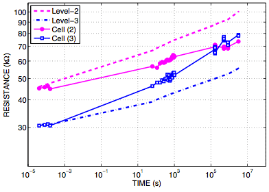
In addition, depending on the voltage, more or less material between the electrodes will undergo a phase change, which directly affects the cell’s resistance. Scientists exploit that aspect to store not only one bit, but multiple bits per cell. In the present work, IBM scientists used four distinct resistance levels to store the bit combinations “00”, “01” 10” and “11”. To achieve the demonstrated reliability, crucial technical advancements in the “read” and “write” process were necessary. “We apply a voltage pulse based on the deviation from the desired level and then measure the resistance. If the desired level of resistance is not achieved, we apply another voltage pulse and measure again – until we achieve the exact level,” explains Pozidis. Despite using the iterative process, the scientists achieved a worst-case write latency of about 10 microseconds, which represents a 100x performance increase over even the most advanced Flash memory on the market today. For demonstrating reliable read-out of data bits, the scientists needed to tackle the problem of resistance drift. Because of structural relaxation of the atoms in the amorphous state, the resistance increases over time after the phase change, eventually causing errors in the read-out. To overcome that issue, the IBM scientists applied an advanced modulation coding technique that is inherently drift-tolerant. The modulation coding technique is based on the fact that, on average, the relative order of programmed cells with different resistance levels does not change due to drift.
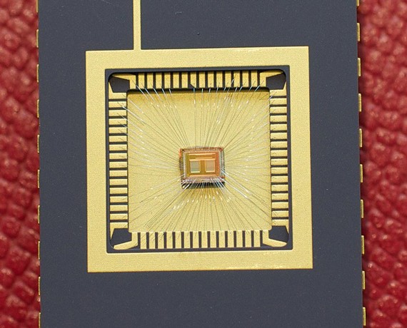
The PCM test chip was designed and fabricated by scientists and engineers located in Burlington, Vermont; Yorktown Heights, New York and in Zurich. This retention experiment has been under way for more than five months, indicating that multi-bit PCM can achieve a level of reliability that is suitable for practical applications. The PCM research project at IBM Research – Zurich will continue to be studied at the recently opened Binnig and Rohrer Nanotechnology Center. The center, which is jointly operated by IBM and ETH Zurich as part of a strategic partnership in nanosciences, offers a cutting-edge infrastructure, including a large cleanroom for micro- and nanofabrication as well as six “noise-free” labs, especially shielded laboratories for highly sensitive experiments.
[ttjad keyword=”general”]





This sounds really BIG! Looking fwd to seeing what comes from it.